Caching in Modern Microprocessors

The modern microprocessors have a speed of 3GHz vs the main memory (RAM) has a speed of 133 MHz. With the newest advancements in hardware, the memory bandwidth only increased between DDR to DDR2 and DDR3 but the latency decrease by a very little factor. Caches were introduced as a level of indirection in order to hide the latency gap.  Caches work on two very important principles of data access patterns:

  1. Spatial Locality: if a memory location is accessed, the nearby memory location is most probably accessed, example: arrays
  2. Temporal Locality: if memory location is accessed, there is probability that the same location will be accessed again, example: loops

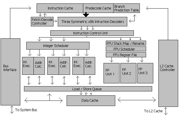
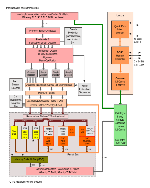
Modern x86 processors have the hierarchy of an L1, L2 and a distributed LLC accessed via the on-die scalable ring architecture. L1 and L2 cache are private to the core and the LLC is shared within all the cores.

  • The Access Timing in terms of CPU cycles
    • L1 – 4 cycles
    • L2 – 12 cycles
    • LLC – 26 to 31 cycles

  • The cache size
    • L1 32 KB data cache (L1I) + 32 KB instruction cache (L1D)
    • L2 – 256 KB

    • LLC – 8 MB to 56 MB.
  • Cache line
    • It is unit of transport between memory.
    • on x86 the cache line size is 64 bytes
  • Data Prefetchers
    • spatial prefetcher attempts to complete every cache line fetched to the L2 cache with another cache line to fill a 128-byte aligned chunk.

    • streamer prefetcher monitors read requests from the L1D cache and fetches the appropriate data and instructions. Server vendors might use their own designation for L1 and L2 prefetchers

  • Cache Snooping protocols:

    CACHE STATE

    DEFINITION

    STATE DEFINITION

    CACHE LINE EXISTS IN

    M

    Modified

    The cache line is updated relative to memory

    Single core

    E

    Exclusive

    The cache line is consistent with memory

    Single core

    S

    Shared

    The cache line is shared with other cores. (The cache line is consistent with other cores, but may not be consistent with memory)

    Multiple cores

    I

    Invalid

    The cache line is not present in this core L1 or L2

    Multiple cores


Types of Caches

  1. Directly mapped caches:
    • an address can reside only at a particular address in cache.
    • Screen Shot 2018-03-18 at 6.23.01 PM
    • Direct mapping is simple and inexpensive to implement, but if a program accesses 2 blocks that map to the same line repeatedly, the cache begins to thrash back and forth reloading the line over and over again meaning misses are very high.
    • Processor registers use logic as direct mapped.
  2. Fully associative caches
    • any block can go into any line of the cache.
  3. Set-associative caches
    • set associative addresses the problem of possible thrashing in the direct mapping method. It does this by saying that instead of having exactly one line that a block can map to in the cache, we will group a few lines together creating a set. Then a block in memory can map to any one of the lines of a specific set. There is still only one set that the block can map to.
    • Screen Shot 2018-03-18 at 6.25.44 PM

Cache Eviction Policy

There are many algorithms for cache eviction in case of conflict example:

  • FIFO – First in first out
    • keep track of insertion time and evicts block that is oldest.
  • LRU – least recently used
    • keep track of references to the data in cache and data with lowest references will be evicted
  • Random

Cache Flush Policy

When the data is updated in cache, there are following policies for updating main memory with updates to cache. Since the main memory is slow, the update is deferred as much as possible.

  • Write-through:
    • Cache pushes all the changes to the main memory immediately
    • advantages are the implementation is simple and less error prone.
    • disadvantages are requirement of bandwidth because of subsequence writes and also write backs take latency because of slowness of main memory.
    • write-no-allocate:
      • the block is modified in the main memory and not loaded into the cache.
    • write-allocate:
      •  the block is loaded on a write miss, followed by the write-hit action.
  • Write back:
    • the update is deferred as much as possible.

Cache Misses

  • Cold or compulsory misses:
    • Cache misses because of first reference to the block in program
  • Capacity misses:
    • Cache misses because of capacity is not enough.
  • Conflict misses:
    • Cache misses because of conflicting cache location.
  • Coherent misses:
    • The coherence miss count is the number of memory accesses that miss because a cache line that would otherwise be present in the thread’s cache has been invalidated by a write from another thread.
  • Coverage misses:
    • he coverage miss count is the number of memory accesses that miss because a cache line that would otherwise be present in the processor’s cache has been invalidated as a consequence of a directory eviction.

Cache Hierarchy

Image credit: http://www.1024cores.net/home/parallel-computing/cache-oblivious-algorithms?

cpu_cache_structure
Cache hierarchy latency vs capacity.

Translation Lookaside Buffer – TLB

  • The TLB is an other form of cache that stores the virtual to physical mappings of addresses.
  • TLB is fully associative.
  • There are generally 2 levels of TLB and less number of entires (128).
  • When a page fault occurs, the hardware starts address translation. Since the address translation in x86 is 5 level, the hardware start looking into the TLB if the address has been translated recently and if found, the translation returns immediately.
  • If the address is not found in the TLB, the hardware walks through the page tables entries in the main memory in order to find the physical address for that page.


Superscalar Processor Design

Superscalar processors are designed to fetch and issue multiple instructions every machine cycle vs Scalar processors which fetch and issue single instruction every machine cycle.

ISA

  • Instruction set architecture provides a contract between software and hardware i.e between program and the machine.
  • ISA is an abstraction between the hardware implementation and programs can be written with knowledge of ISA.
  • ISA ensures portability.
  • For hardware developers, ISA is a specification.
  • The set of instructions defined by ISA is an assembly language.
  • Dynamic-static interface: defined as separation between stuff can be done statically (at compile time) and stuff can be done dynamically (at runtime).

Processor Performance is measured as CPI – cycles per instruction. There are following techniques for decreasing instruction count

  • Executing multiple instructions per cycle using pipelining. The deeper pipeline goes, the branch misprediction penalty goes high as processor has to flush the pipeline and fill it up with new instructions. Also a deeper pipeline increases hardware and latency overhead.
  • Decreasing the instruction count and moving the complexity on Hardware may increase cycle time.

Stages of Execution in Scalar Pipelined Processors

procsimu-dlx-pipeline
Fetch, Instruction decode, execute, memory and writeback stages in scalar pipelines processors.

Image credit: http://www.oberle.org/procsimu-index.html


Screen Shot 2018-03-17 at 11.31.11 PM
CRAY-1 is an example of superpipelined processor
Screen Shot 2018-03-17 at 11.38.49 PM
Superscalar Instruction level parallelism machines
Screen Shot 2018-03-17 at 11.38.39 PM
Very Long Word Instruction Set Machines

Stages in scalar Pipelined processors

  1. Fetch: Since main memory is slow, the fetch stage is divided into two or more sub-stages. This ensures once the data/instructions starts coming into processor for execution, more than stage is executed in parallel. But since all the next stages are depend upon this stage, the pipeline is stalled until data/instructions become available at this stage. This stage is considered as in-order front-end.
    1. A superscalar processor can fetch more than one instruction in parallel.
  2. Decode: The instructions are divided into further micro-instructions(micro-ops) at this level. Various caching and optimization techniques are done in order to complete this stage faster. This stage is considered as in-order front-end.
    1. for CISC processors this stage is complex and itself is divided into multiple substages.
    2. Since the decoding functionality is extremely complex, the predecoding has been implemented.
  3. Dispatch:
  4. Execution: the execution unit of a processor generally has more parallelism and considered as out of order execution stage. Intel x86 processors have 2 ALU, FPUs and vectorized processors in this stage.
  5. Complete
  6. Retite ( Writeback) : the results of processor execution are written back the registers.

640px-MIPS_Architecture_(Pipelined).svg

Image credit: By Inductiveload – Own work, Public Domain, https://commons.wikimedia.org/w/index.php?curid=5769084

The instruction types are

  1. Arithmetic Operations
  2. Load/store – data movement operations between memory, caches and registers.
  3. Branch Instructions

Superscalar Pipelines

0708.cs-323016
Image credit: http://euler.mat.uson.mx/~havillam/ca/CS323/0708.cs-323009.html

This an example of a super scalar processor design. The pipeline is not only deep but also parallel.

Dynamic Pipelines

figure1
image credit: http://www.cs.utah.edu/~wyman/classes/arch/athlon.html
  • Buffers are used to hold the data between multiple stages in the pipelined design.
  • In parallel pipelined processors, multientry buffers are used.
  • Parallel pipelined design that supports out of order execution of instructions is called as dynamic pipeline.
  • The complex multientry buffer designs allow instructions flow in different order.
    • First of the buffers in pipeline is dispatch buffer. This buffer receives instructions from program in order but can dispatch them out of order to the functional units.
    • Similar kind of buffer named completion buffer is present at the back end of pipeline. It can receive results of computation in any order. This buffer retires the instructions in order and proceeds the results to WB stage.

Buffers in superscalar design

haswell-5
Image credit: https://www.realworldtech.com/haswell-cpu/6/

Example of latest Intel x86 Microprocessor

Each core has following number of hardware units:

  • Reorder Buffer
    • ROB is used for register renaming and reordering the out of order execution results
    • 192 entries
  • Reservation Station
    • has 60 entries
  • Register file
    • 168 integer registers
  • Vector registers
    • 168
  • Loopback buffer
    • 56 entries.
  • μop cache
    • 1536 μops, 8 way, 6 μop line size, per core
  • L1I cache
    • 32 KB, 8 way set associative 64 sets
    • 64 bytes cache line
    • 32 bytes read and write per clock cycle
  • L1D cache
    • 32 KB, 8 way set associative 64 sets
    • 64 bytes cache line
  • L2 cache
    • 256KB, 8 way set associative 512 sets
    • 64 bytes cache line
  • L3 cache
    • 45 MB (ring shaped shared)
  • Instruction Fetch Rate
    • 16 bytes per clock cycle.

Trace Cache

After the instructions fetch, they are decoded and divided into μops. Instructions are stored in the trace cache after being decoded into μops. The opcode has length between 1 to 15.

Here is a nice video about breaking ISA instruction set.

Branch Prediction Techniques

Predicting branches correctly is important for superscalar processor performance. The branch prediction is much predictable because of various techniques explained below:

  • Branch Target Speculation
    • A fully associative cache name Branch Target buffer is used for storing target address of last branch taken. For next lookup, the cache is used.
    • image007image009
  • Branch Conditional Speculation
  • Multi-level adaptive branch predictor
  • Image13
    • The Two-Level Branch Predictor, also referred to as Correlation-Based Branch Predictor, uses a two-dimensional table of counters, also called “Pattern History Table”. It was introduced by Yeh and Patt who because of the fact that the outcome of the branch depends not only on the branch address but also on the outcome of other recent branches (inter branch correlation) and a longer history of the same branch itself (intra branch correlation).
      • A Global Branch History is a shift register in which the outcome of any branch is stored. A “one” is stored for a taken branch and a “zero” for a non-taken one. The register is shifted through while storing the newest value. In order to address the table, the n last branch outcomes are considered.
      • The Local History Table is a table of shift registers of the sort of a global branch history. Each shift register, however, refers to the last outcomes of one single branch. Since this local history table is accessed as a one-level branch prediction table, it is not guaranteed that no overlapping of the branches occurs, and in one shift register may be stored the information of different branches.
      • Since the table has only two dimensions, two of the three information sources have to be selected to access rows and columns. Another method is to merge two sources to one, which will be covered later.
      • In general it can be stated that a two-level branch predictor is more accurate than a one-level branch predictor, but this advantage is also associated with the disadvantage of a more costly implementation and the fact that the so called Warm Up Phase, i.e. the time the table entries contain usable values, is much longer.
  • Static Branch Prediction

    • Static Branch prediction algorithms do not speculate the prediction based on the past hence they are simple. Following are some of the techniques
  • Dynamic Branch Prediction

    • Dynamic Branch prediction predicts at the rate of 80% to 95%.
    • The past outcomes are used as input for branch prediction.
      • One level branch predictor
      • Various predictor features
      • Two level branch predictor
      • Hashing techniques
      • Difficulties
      • Hybrid branch predictor
      • Multiple component Hybrid branch predictor
      • Branch classification
      • Industry branch prediction implementations

Register Renaming

Register renaming is controlled by the reorder buffer and the scheduler. Register renaming is a technique that eliminates the false data dependencies arising from the reuse of architectural registers by successive instructions that do not have any real data dependencies between them.

Machine language programs specify reads and writes to a limited set of registers specified by the instruction set architecture (ISA). For instance, the Alpha ISA specifies 32 integer registers, each 64 bits wide, and 32 floating-point registers, each 64 bits wide. These are the architectural registers


Modern Microprocessors

Characteristics of Modern Microprocessors

  • Multicore processors: Modern processors can have between 2 (LCC- Low core count) to 24 (HCC – high core count) number of cores for parallelism at hardware level.
  • out-of-order execution:
    • In order to hide the ever widing gap between the CPU and main memory, all modern CPUs are pipelined and have execution reordering.
    • While CPU is waiting for some data or instructions from memory, it might work on something else. There is a complex logic designed in hardware to check the input dependencies between instructions.
  • Multi-level caches: There are atleast 3 levels of caches built in the processor which acts like local memory to the CPU.
  • Speculative execution: Modern CPUs predict the memory location of data to next instruction that may be executed.
  • Microops: The assembly instructions are divided into micro operations which makes it easy for execution and the result is then combined into one.
  • Register renaming: The compilers can compile the code with logical registers like EAX, EBX, EDX etc. The processors have a lot of temporary registers. So it renames one of its temporary registers with logical names.

Architecture diagram for Intel Nehalem Processor

Intel_Nehalem_arch

Image credit: By Appaloosa (Own work) [GFDL (http://www.gnu.org/copyleft/fdl.html) or CC-BY-SA-3.0 (http://creativecommons.org/licenses/by-sa/3.0/)%5D, via Wikimedia Commons

CPU Package Overview

Screen Shot 2018-03-15 at 12.00.58 AM

Image credit: http://pages.rubrik.com/rs/794-OHF-673/images/vSphere_6.5_Host_Resources_Deep_Dive.pdf

Intel Xeon Uncore Elements

UNCORE ELEMENT

DESCRIPTION

RESPONSIBLE FOR

QPI Agent

Quick Path Interconnect

QPI caching agent, manages R3QPI and QPI Link Interface.

PCU

Power Controller

Core/Uncore power unit and thermal manager, governs P-State of the CPU, C-State of the Core and package. It enables Turbo Mode and can throttle cores when a thermal violation occurs.

Ubox

System Config Controller

Intermediary for interrupt traffic between system and core.

IIO

Integrated IO

Provides the interface to PCIe Devices.

R2PCI

Ring to PCI Interface

Provides interface to the ring for PCIe access.

IMC

Integrated Memory Controller

Provides the interface to RAM and communicates with Uncore through Home Agent.

HA

Home Agent

Responsible for ordering read/writes coming from Ring to IMC. Provides directory cache coherency.

SMI

Scalable Memory Interface

Provides IMC access to DIMMs.

High Core Count Architecture

Screen Shot 2018-03-15 at 12.04.59 AM.png

Image Credit: http://pages.rubrik.com/rs/794-OHF-673/images/vSphere_6.5_Host_Resources_Deep_Dive.pdf

Intel Xeon Processor Overview

GENERATION

BRANDING

YEAR

PROCESS

CADENCE

MAX CORES

Nehalem

X5500

2008

45nm

4

Westmere

X5600

2010

32nm

Tick

6

Sandy Bridge

E5-2600-v1

2012

32nm

Tock

8

Ivy Bridge

E5-2600-v2

2013

22nm

Tick

12

Haswell

E5-2600-v3

2014

22nm

Tock

18

Broadwell

E5-2600-v4

2016

14nm

Tick-Progress

22

Skylake

2P

2017

14nm

Architecture

28

Image Credit: http://pages.rubrik.com/rs/794-OHF-673/images/vSphere_6.5_Host_Resources_Deep_Dive.pdf